


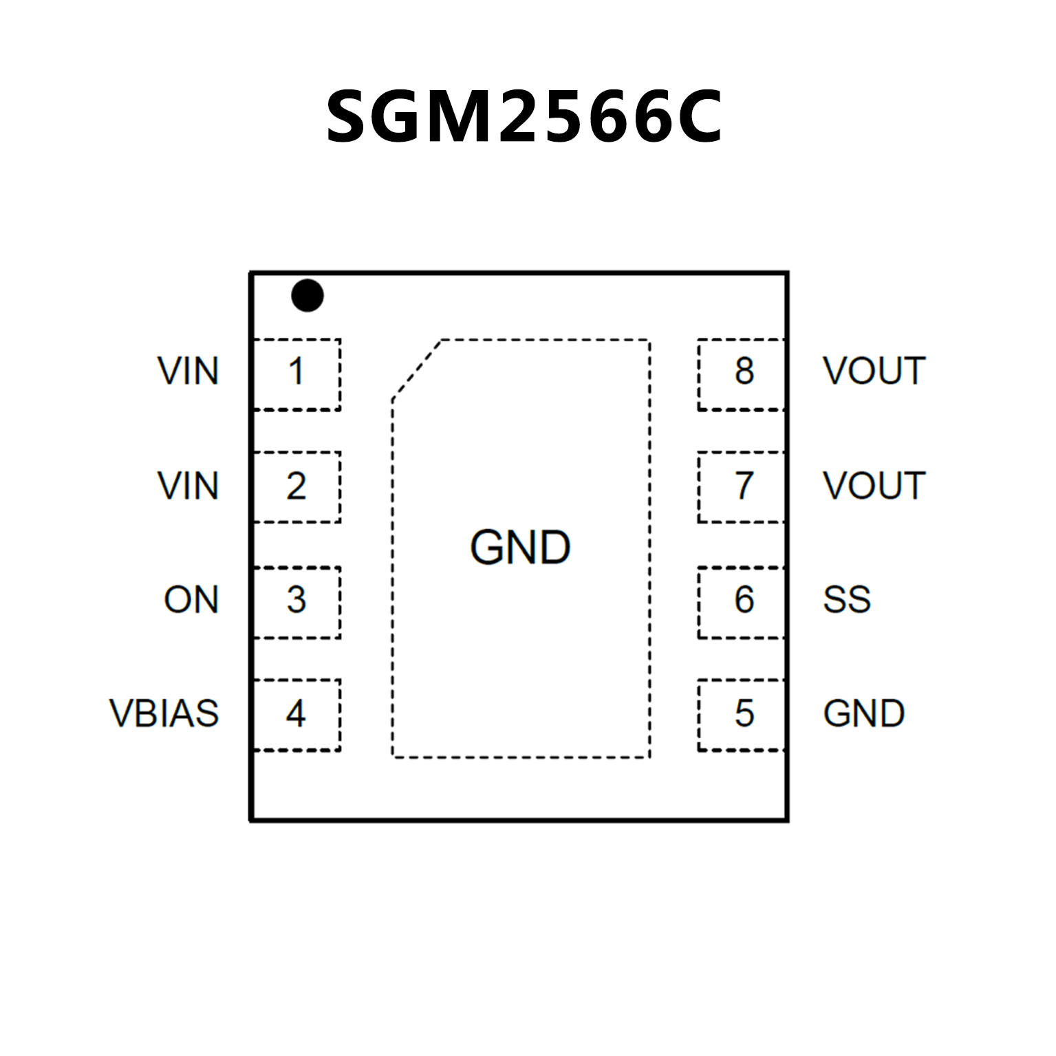
 SGM2566C.pdf
? Input Voltage Range: 0.6V to VBIAS
? VBIAS Voltage Range: 2.5V to 5.7V
? Ultra-Low On-Resistance: 14m? (TYP)
? Maximum Continuous Load Current: 5A
? Quiescent Current: 11μA (TYP)
? Thermal Shutdown
? Programmable Output Ramp Time
? Support with 1.2V, 1.8V, 2.5V and 3.3V GPIOs
? Quick Output Discharge
? -40℃ to +105℃ Operating Temperature Range
? Available in a Green TDFN-2×2-8AL Package-8AL Package
? Input Voltage Range: 0.65 V to 3.6 V
RON = 9.2 mΩ at VIN = 3.6 V
RON = 9.2 mΩ at VIN = 1.8 V
RON = 10.2 mΩ at VIN = 1 V
RON = 13.1 mΩ at VIN = 0.65 V
? 3-A Maximum Continuous Switch Current
? Quiescent Current, IQ,VIN = 29 μA at VIN = 3.6 V
? Low Control Input Threshold Enables
1.5-, 1.8-, 2.5-, or 3.3-V Logic
? Controlled Slew Rate
tR = 97 μs at VIN = 3.6 V (TPS22925Bx)
tR = 810 μs at VIN = 3.6 V (TPS22925Cx)
? Reverse Current Blocking (When Disabled)
? Quick Output Discharge (QOD)
(TPS22925B and TPS22925C only)
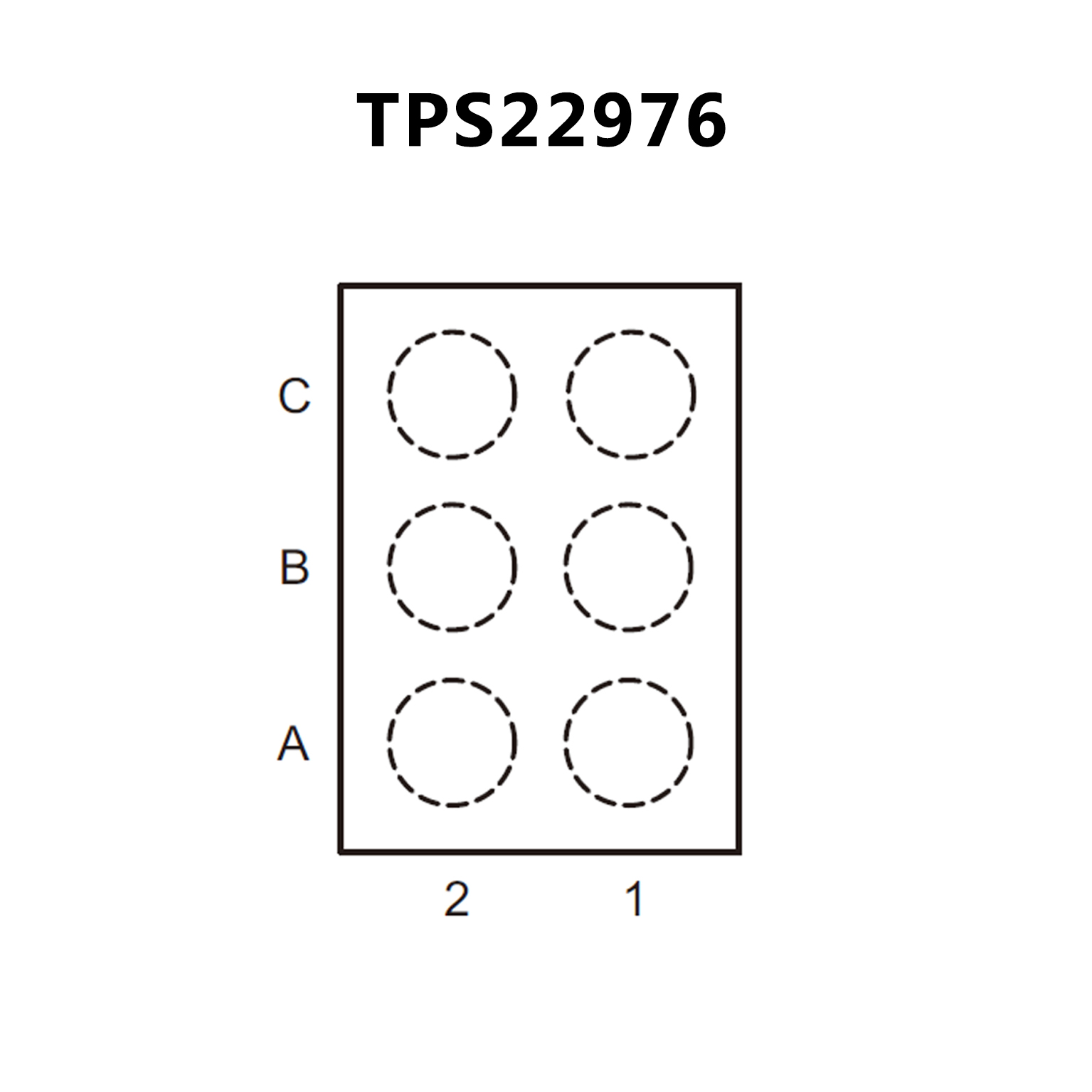
? Wafer Chip Scale Package:
0.9 mm x 1.4 mm, 0.5-mm Pitch, 0.4-mm Height
? ESD Performance Tested per JESD 22
2-kV HBM and 1-kV CDM