


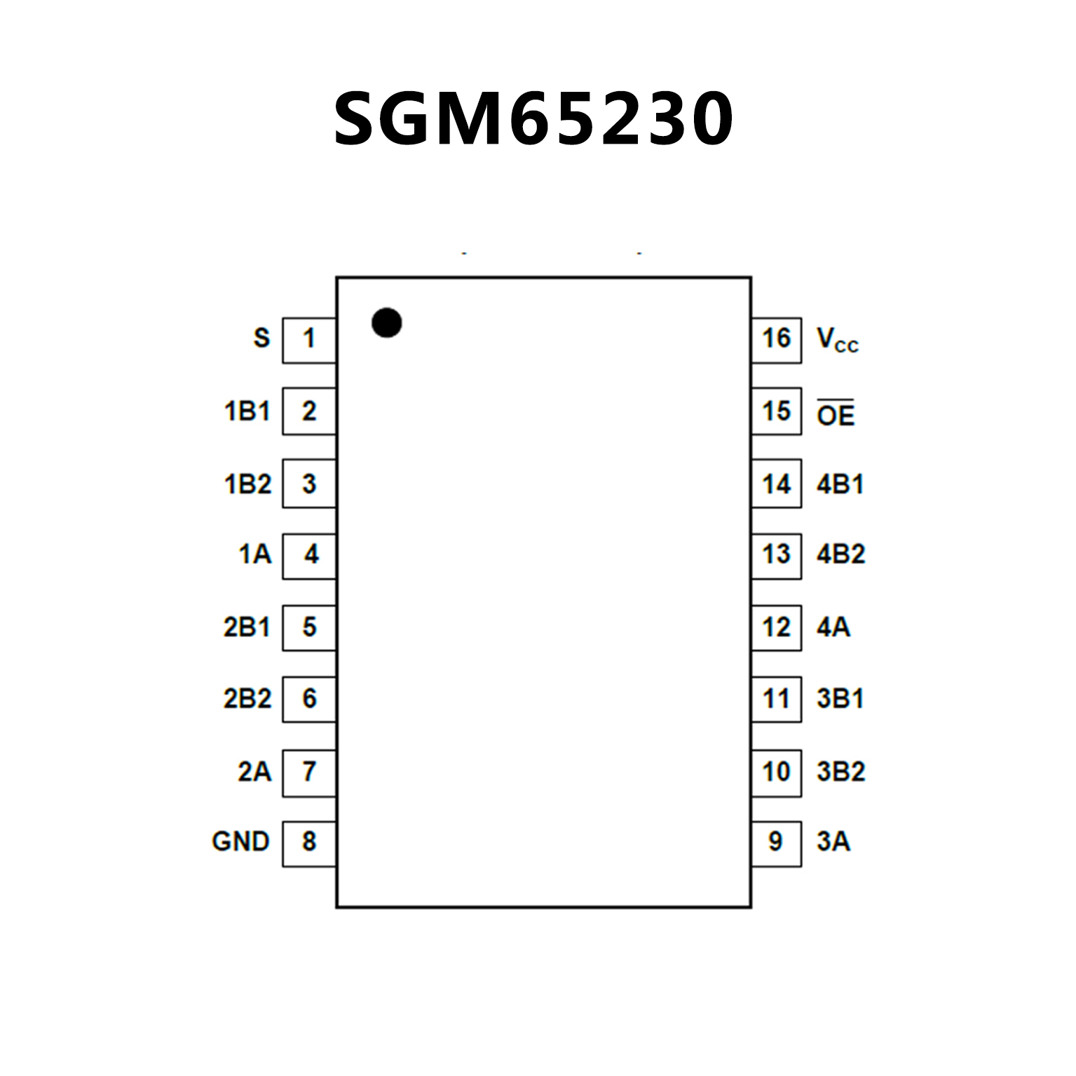
 SGM65230.pdf
? High-Bandwidth Data Path (Up to 400MHz)
? 5V Tolerant I/Os with Device
Powered Up or Powered Down
? Low and Flat On-Resistance
(RON) Characteristics with 3.3V VCC: 4Ω (TYP)
? Rail-to-Rail Switching on Data I/O Ports
0V to 5V Signal Passing with 3.3V VCC
0V to 3.3V Signal Passing with 2.5V VCC
? Bidirectional Data Flow
? Low Input/Output Capacitance
Minimizes Loading and Signal
Distortion: CIO(OFF) = 7pF (TYP)
? Fast Switching Frequency: fOE = 20MHz (TYP)
? Data and Control Inputs Provide Undershoot Clamp Diodes
? Low Power Consumption: ICC = 0.6mA (TYP)
? VCC Operating Range from 2.3V to 3.6V
? Data I/Os Support 0V to 5V Signaling Levels:
(0.8V, 1.2V, 1.5V, 1.8V, 2.5V, 3.3V, 5V)
? Control Inputs Can Be Driven by
TTL or 5V/3.3V CMOS Outputs
? IOFF Supports Partial-Power-Down Mode Operation
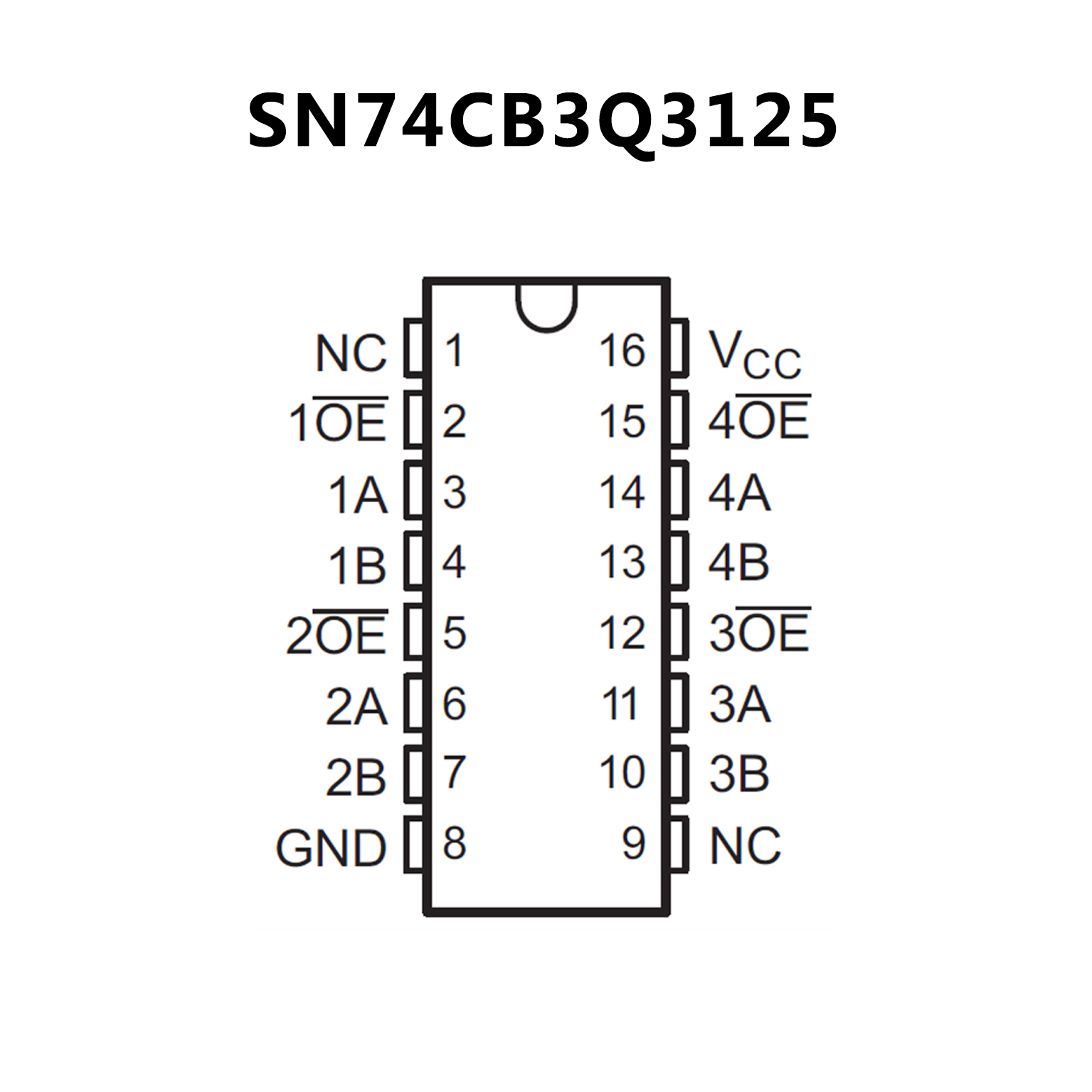
? Available in a Green TSSOP-16 Package
? High-Bandwidth Data Path (up to 500 MHz(1))
? 5-V Tolerant I/Os With Device Powered Up or
Powered Down
? Low and Flat ON-State Resistance
(ron) Characteristics Over Operating Range
(ron = 3 ? Typ)
? Rail-to-Rail Switching on Data I/O Ports
0-V to 5-V Switching With 3.3-V VCC
0-V to 3.3-V Switching With 2.5-V VCC
? Bidirectional Data Flow With
Near-Zero Propagation Delay
? Low Input and Output Capacitance
Minimizes Loading and Signal Distortion
(Cio(OFF) = 4 pF Typ)Fast Switching
Frequency (fOE = 20 MHz Max)
Data and Control Inputs Provide
Undershoot Clamp Diodes
Low Power Consumption
(ICC = 0.3 mA Typ)
? VCC Operating Range From 2.3 V to 3.6 V
? Data I/Os Support 0-V to 5-V Signaling Levels
(0.8 V, 1.2 V, 1.5 V, 1.8 V, 2.5 V, 3.3 V, 5 V)
? Control Inputs Can Be Driven by TTL,
5-V, or 3.3-V CMOS Outputs
Ioff Supports Partial-Power-Down Mode
Operation Latch-Up Performance
Exceeds 100 mA Per JESD 78, Class II
? ESD Performance Tested Per JESD 22
2000-V Human-Body Model
(A114-B, Class II)
? 1000-V Charged-Device Model (C101)
?Supports Both Digital and Analog
Applications: USB Interface, Differential
Signal Interface, Bus Isolation, Low-Distortion Signal Gating